
PCB Manufacturing Services
We deliver high-precision PCB manufacturing tailored to your exact specifications, ensuring reliability, performance, and compliance with industry standards. Whether you need prototypes for R&D or high-volume production, our advanced fabrication capabilities support rigid, flex, and rigid-flex PCBs with tight tolerances and superior quality. From quick-turn prototypes to complex multi-layer boards, we leverage cutting-edge technology and rigorous testing to meet the demands of aerospace, medical, automotive, and industrial applications.
- Prototype PCB Fabrication – Fast-turnaround boards for testing and validation
- High-Volume PCB Production – Scalable manufacturing with consistent quality
- Multi-Layer PCBs (Up to 32 Layers) – High-density designs for complex applications
- HDI (High-Density Interconnect) PCBs – Microvias and fine-pitch traces for compact electronics
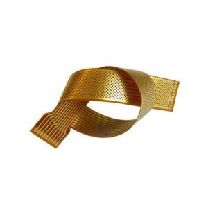
- Flex & Rigid-Flex PCBs – Durable, lightweight solutions for dynamic applications
- Heavy Copper PCBs (Up to 20oz) – High-current and power electronics support
- RF/Microwave PCBs – Low-loss materials for high-frequency applications
- Aluminum & Metal-Core PCBs – Superior thermal management for LEDs and power devices
- Impedance-Controlled PCBs – Precision signal integrity for high-speed designs
- PCB Fabrication with Special Finishes – ENIG, HASL, Immersion Silver, OSP, and more
Precision Manufacturing for Every Stage of Development
Our end-to-end PCB manufacturing services bridge the gap between design and deployment, offering seamless scalability from first prototypes to mass production. Leveraging automated optical inspection (AOI), impedance testing, and 100% electrical verification, we ensure every board—whether a 2-layer prototype or 32-layer HDI—meets exacting performance criteria. For mission-critical applications, we provide specialized solutions like RF/microwave boards with Rogers materials and metal-core PCBs with active thermal management, all manufactured under IPC-6012 Class 3 standards. With 48-hour quick-turn options and dedicated engineering support, we accelerate your time-to-market without compromising the reliability demanded by medical, aerospace, and defense industries.
Why Choose Us
- Professional Services: From design to delivery, there is a person in charge of managing your project.
- Stringent Fabrication Processes: The production line features multiple inspection points and our operators strictly adhere to rigorous quality management regulations to ensure the highest level of quality.
- IPC & ISO Certified Manufacturing: All PCBs are manufactured to meet stringent IPC-A-600 Class 2/3 and ISO 9001:2015 standards, with compliance levels tailored to customer requirements.
- Advanced Equipment: Debarring machine, double-sided alkaline etching machine, metal chemical cleaning machine, etching production line and more.
- Large Production Capacity: UMO Technology operates factories in both Shenzhen and Huizhou, with a combined capacity of over 500,000 units.
- No Minimum Order Quantity: Offer PCB prototyping services with no minimum order quantity requirement, ensuring that even small-scale projects receive the same meticulous attention to detail as our larger orders.
- Competitive Pricing: Our focus on long-term partnerships and a win-win approach allows us to provide cheap PCB fabrication services without compromising on quality.

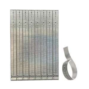
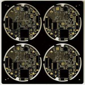
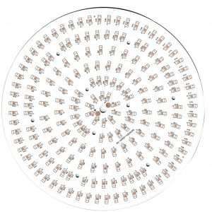
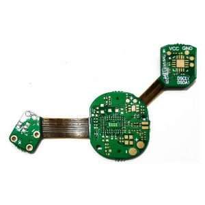
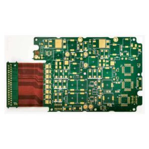
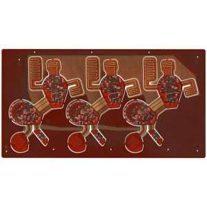
Bare Board Production Samples
PCB Manufacturing Capabilities
We combine precision engineering with cutting-edge technology to deliver PCBs that meet your exact specifications. Whether you need prototypes or full-scale production, our advanced manufacturing processes ensure quality, reliability, and performance—backed by rigorous testing and certifications.
Refer to the table below for detailed technical specifications and capabilities.
| Item | Copper Weight (oz) | mm | mil |
|---|---|---|---|
| Minimum Track Width/Spacing | 1oz | 2-Layers : 0.1mm/0.1mm Multi-Layer: 0.09mm/0.09mm BGA fanout: 0.08mm/0.08mm | 2-Layers : 4mil/4mil Multi-Layer: 3.5mil/3.5mil BGA Fanout: 3mil/3mil |
| 2oz | 2-Layers : 0.16mm/0.16mm Multi-Layer: 0.16mm/0.2mm | 2-Layers : 6.5mil/6.5mil Multi-Layer: 6.5mil/8mil | |
| Track width tolerance | ±20% | ||
| Plated Through Hole (PTH) Minimum Annular Ring | 1oz | 2-Layers : Typical 0.254mm, Minumum 0.18mm Multi-Layer : Typical 0.2mm, Minumum 0.15mm | 2-Layers : Typical 10mil, Minumum 7mil Multi-Layer : Typical 8mil, Minumum 6mil |
| 2oz | 2-Layers : 0.254mm Multi-Layer : 0.254mm | 2-Layers : 10mil Multi-Layer : 10mil | |
| Non-Plated Through Hole (NPTH) Minimum Annular Ring | - | ≧0.45mm | ≧18mil |
| Minimum Same-Net Track Spacing | - | 0.254mm | 10mil |
| Minimum BGA Pad to Track Spacing | - | 0.09mm | 3.5mil |
| Minimum BGA Pad Diameter | - | 0.254 | 10mil |
| Hatched Grid Width/Spacing | - | 0.254 | 10mil |
| Minimum Via Hole to Inner Layers Copper Spacing | - | 0.2mm | 8mil |
| Minimum Via Hole to Track Spacing | - | 0.2mm | 8mil |
| Minimum PTH Hole to Inner Layers Copper Spacing | - | 0.3mm | 12mil |
| Minimum PTH Hole to Track Spacing | - | Typpical: 0.35mm Worst Cases: 0.28 | Typpical: 14mil Worst Cases: 11mil |
| Minimum NPTH Hole to Track Spacing | - | 0.2 | 8mil |
| Minimum SMD Pad to Pad Clearance | - | 0.15mm for 0402 Pads. Larger Pads need more spacing. | 6mil |
| Manufacturing Dimensions | Capability | Note |
|---|---|---|
| Maximum Dimensions | FR4 Thickness ≥ 0.8mm : 670 x 600 mm FR4 Thickness < 0.8mm : 600 x 500 mm 2-Layer FR4 : 1000 x 600 mm Aluminum : 600 x 500 mm Copper PCB : 480 x 280 mm | |
| Minimum Dimensions | PCB Thickness ≥ 0.6mm : 3 x 3 mm | Call for thinner PCBs |
| Dimension Tolerance | ±0.1mm | |
| Board Thickness (mm) | Less than 12-Layers: 0.5, 0.6, 0.8, 1.2, 1.6 and 2.0 mm 12-Layers and more : ≥ 2.5mm | |
| Thickness Tolerance when T>1.0 mm | ±10% x T | |
| Thickness Tolerance when T≤1.0 mm | ±0.1mm | |
| Finished Outer Layer Copper | 1oz or 2oz | Including Plating |
| Finished Inner Layer Copper | 0.5oz by Default | 1oz or 2oz are also available |
| Panel Size (mm) | xxx | |
| Bow And Twist | ≤0.75% |
| Manufacturing Materials | Capability | Notes |
|---|---|---|
| FR4, Halogen-Free FR4 | Grade A materials from Nan Ya, KB, Shengyi, and other top-tier suppliers | Tg: 135C, 150C, 170C, etc. |
| Ceramic Filling High Frequency Material | Rogers 4003C/4350B | |
| PTFE High Frequency Material | Rogers Series, Arlon Series, Taconic Series, F4BM Series | |
| Special PP | NFPP: Arlon 49 N, VT47 Ceramic Filling PP: Rogers 4450F PTFE PP: Arlon 6700, Taconic FR-27 | |
| Rigid PI Material | Arlon 85 N, VT901 | |
| Metal Core | 1-Layer Aluminum and Copper Cores | |
| Material Mixed Laminate | 4 layers – 10 layers (FR4 + Ro4350, FR4 + Aluminium, FR4 + FPC) | |
| Note | Other special materials can be processed and produced by means of customer supply or purchasing. |
| Package (Imperail) | 0402 | 0603 | 0805 | 1206 | QFN | QFP | SOP/SOIC | SOT23, SOT-363, etc. |
|---|---|---|---|---|---|---|---|---|
| 0402 | 0.15mm (6mil) | 0.18mm (7mil) | 0.20mm (8mil) | 0.25mm (10mil) | 1mm (40mil) | 0.5mm (20mil) | 0.4mm (16mil) | 0.2mm (8mil) |
| 0603 | 0.18mm (7mil) | 0.18mm (7mil) | 0.25mm (10mil) | 1mm (40mil) | 0.5mm (20mil) | 0.4mm (16mil) | 0.20mm (8mil) | |
| 0805 | 0.18mm (7mil) | 0.25mm (10mil) | 1mm (40mil) | 0.5mm (20mil) | 0.4mm (16mil) | 0.20mm (8mil) | ||
| 1206 | 0.35mm (14mil) | 1mm (40mil) | 0.5mm (20mil) | 0.4mm (16mil) | 0.20mm (8mil) | |||
| QFN | 1mm (40mil) | 1mm (40mil) | 1mm (40mil) | 1mm (40mil) | ||||
| QFP | 1.25mm (50mil) | 1.25mm (50mil) | 1mm (40mil) | |||||
| SOP/SOIC | 0.5mm (20mil) | 0.4mm (16mil) | ||||||
| SOT-23, SOT-363, etc. | 0.4mm (16mil) |
| Drilling Parameter | mm | mil | Note |
|---|---|---|---|
| Drill Diameter | 0.15-6.3mm | 6-250mil | Greater holes can be made by hole expansion process |
| Plated Hole Diameter Tolerance | -0.08mm to +0.13mm | -3mil to 5mil | |
| Minimum Non-Plated Hole Size | 0.5mm | 20mil | NPTH should be Marked in Mechanical gerber file |
| Non-Plated Hole Diameter Tolerance | ±0.2mm | ±8mil | |
| Average Hole Plating Thickness | 0.018mm | 0.7mil | |
| Minimum Via Hole Size | 0.15mm | 6mil | Use 0.2mm whenever possible |
| Minimum Via Diameter | 0.25mm | 10mil | Via diameter should be 0.1mm(0.15mm preferred) larger than Via hole size. |
| Minimum Non-Plated Slot Width | 1.0mm | 40mil | |
| Minimum Plated Slot Width | 0.5mm | 20mil | |
| Minimum Via Hole to Hole Spacing | 0.2mm | 8mil | |
| Minimum Pad Hole to Hole Spacing | 0.45mm | 18mil | |
| Minimum Castellated Hole Diameter | 0.5mm | 20mil | |
| Minimum Castellated Hole to Board Edge Spacing | 1.0mm | 40mil | Edges that do not have Casellated holes |
| Minimum Castellated Hole to Hole Spacing | 0.5mm | 20mil |
| Item | Standard | Advanced | Innovative | |
|---|---|---|---|---|
| Tin Lead HASL | Leaded Hot Air Solder Leveling | FR4, Aluminum Cores | A cost-effective PCB surface finish where molten solder is applied to pads, then leveled with hot air. | ✔ Consumer electronics ✔ High-volume orders ✔ Non-fine-pitch components |
| Lead-Free HASL | Lead-Free Hot Air Solder Leveling | FR4, Aluminum Cores | A cost-effective PCB surface finish where molten Lead-Free solder is applied to pads, then leveled with hot air. | ✔ Consumer electronics ✔ High-volume orders ✔ Non-fine-pitch components |
| ENIG | Electroless Nickel Immersion Gold | FR4 and High-Freq Boards | A premium PCB surface finish with a nickel barrier layer and thin gold coating for reliable protection and connectivity. | ✔ High-density designs (HDI, <0.5mm BGA pitch) ✔ Harsh environments (high humidity/temperature) ✔ Gold wire bonding (RF/medical devices) |
ENEPIG | Electroless Nickel Electroless Palladium Immersion Gold | Harsh environment electronics | An advanced, ultra-reliable surface finish combining nickel, palladium, and gold layers for superior performance in demanding applications. | ✔ Gold & Palladium Protection – Prevents nickel corrosion ("black pad" risk) ✔ Wire-Bondable – Supports both gold and aluminum bonding ✔ Lead-Free & RoHS Compliant ✔ Flat Surface – Ideal for fine-pitch/BGA components |
| Hard Gold | Electrolytic Hard Gold | FR4 and High-Freq Boards with Edge connectors or probe contacts | An ultra-durable surface finish with thick gold layer (typically 5-50μm) over nickel, ideal for high-wear applications. | ✔ Exceptional wear resistance – Withstands 10,000+ insertion cycles ✔ Reliable conductivity – Low contact resistance ✔ High-temperature stable – For harsh environments ✔ Wire-bondable – Critical for RF/medical devices |
| ISn | Immersion Tin | HDI Boards | A flat, solderable surface finish where a thin layer of tin is chemically deposited on copper pads, ideal for fine-pitch applications. | ✔ Excellent flatness – Perfect for <0.3mm pitch/BGA ✔ Lead-free & RoHS compliant ✔ Cost-effective – Mid-range pricing |
| OSP (um) | Organic Solderability Preservative | Copper Cores only | A thin, organic coating applied to copper pads to prevent oxidation while maintaining solderability. | ✔ Cost-effective (budget-friendly option) ✔ Flat surface – Ideal for fine-pitch components ✔ Lead-free & RoHS compliant ✔ Simple process – Easy to apply and rework |
| Solder Mask Parameter | mm | mil | Notes |
|---|---|---|---|
| Minimum Solder Mask Expansion | 0.038mm | 1.5mil | Keep at least 0.05mm Spacing between Solder Mask Opening and tracks |
| Soldermask bridge | 2-Layer (1oz): 0.2mm (0.23mm for Black, White) Multi-Layer (1oz): 0.1mm (0.13mm for Black, White) | 2-Layer (1oz): 8mil (9mil for Black, White) Multi-Layer (1oz): 4mil (5mil for Black, White) | The other colors are Green, Red, Yellow, Blue and Purple |
| Solder mask dielectric constant | 3.8 | - | |
| Solder mask ink thickness | ≥ 10μm | - | |
| Via Filling with Solder Mask | - | - | ✔ Filled vias must not have soldermask openings on either side ✔ Filled vias should have ≥ 0.35 mm clearance from other soldermask openings (e.g. pads) ✔ Filled vias must be no wider than 0.5 mm diameter |
| Legend Parameters | mm | mil | Note |
|---|---|---|---|
| Minimum Line Width | 0.15mm | 6mil | Lower width may cause illegible character |
| Minimum Text Height | 1.0mm | 40mil | Lower Height may cause illegible character |
| Character Width to Height Ratio | 1:6 | 1:6 | Keep this ratio wherever possible |
| Minimum Pad To Silkscreen | 0.15mm | 6mil |
| Cutting Parameters | mm | mil | Note |
|---|---|---|---|
| Minimum Copper to V-Cut Spacing | 0.4mm | 16mil | |
| V-Cut Dimensions Tolerance | ±0.4mm | ±16mil | PCB thickness ≥ 0.6 mm |
| V-Cut Groove Angle | 25° | ||
| Minimum Copper to Routed Spacing | 0.2mm | 8mil | |
| Routed Dimensions Tolerance | ±0.2mm | ±8mil | |
| Minimum Copper to Non-Mouse-Bite Board Edge | 0.2mm | 8mil | |
| Mouse Bites Panel Spacing (Moise Bite Edge) | 1.6mm to 2mm | 63mil to 79mil | |
| Recommended Mouse Bite Hole Diameter | 0.5mm to 0.8mm | 20mil to 32 | |
| Recommended Mouse Bite Holes Spacing | 0.2mm to 0.3mm | 8mil to 12mil | |
| Minimum Mouse Bite Tab Width | 5mm | 200mil |
| Special Process | Availability | Description |
|---|---|---|
| Back Drilling | Yes | Removes unused copper stubs from through-holes, Essential for high-frequency designs to: ✔ Reduce signal distortion ✔ Improve high-speed performance ✔ Eliminate EMI risks |
| HDI PCB with Blind/Burried Via | Yes | Enable high-density routing in multilayer boards: ✔ Blind: Connects outer to inner layers ✔ Buried: Links inner layers only ✔ Saves space, improves signal integrity |
| Edge Plating | ✔Minimum PCB Thickness: 0.6mm ✔Minimum PCB Size: 10x10mm ✔Three or more 3mm breaks are required | Protects and conducts on board edges: ✔ Reinforces connector areas ✔ Enhances ground shielding ✔ Prevents delamination |
| Plated Half Holes | Yes | Enable board-to-board connections: ✔ Create castellated edges ✔ Allow direct soldering ✔ Save assembly space |
| Hybrid Material Lamination | Essential for RF, power, and high-speed designs. 4 layers – 10 layers (FR4 + Ro4350, FR4 + Aluminium, FR4 + FPC) | |