
Consumer PCB Manufacturing: From Design to Assembly
- High-Volume PCBA for Mass Market Innovation
- Cost-optimized designs for smart home/IoT devices
- Rapid prototyping to accelerate product launches
- Aesthetic-conscious miniaturization (flex PCBs, ultra-thin designs)
High-Volume Consumer PCBs: Fast, Affordable & Market-Ready
We specialize in cost-optimized PCB manufacturing for consumer electronics, from smart home devices to wearables. Our streamlined design-for-manufacturing (DFM) process and Asian supply chain partnerships ensure rapid prototyping and high-volume production—balancing quality with aggressive pricing to keep your products competitive.
Beyond Basic: Premium PCBs for Consumer Electronics
The term ‘consumer-grade’ often implies lower quality, but our PCB manufacturing breaks this stereotype. By adhering to IPC Class 2/3 standards—including proper solder mask application, copper weight specifications, and thorough electrical testing—we ensure mass-market devices achieve exceptional reliability. Whether producing PCBs for IoT sensors, home appliances, or personal electronics, we implement design-for-reliability (DFR) practices that address common failure points like thermal stress and mechanical wear. The result: cost-effective boards that withstand real-world usage while meeting tight consumer electronics margins.
Consumer PCB Trends
The consumer electronics market is expected to reach $705 billion by 2030, driving significant demand for electronic products worldwide. As a result, the PCBA industry for consumer electronics is rapidly expanding globally. High-quality printed circuit boards are essential for the efficient operation and functional realization of electronic products. Furthermore, changing consumer demand for electronic products is driving new trends in the PCBA industry, and UMO Technology is committed to providing customers with insights into these trends.
High Density Interconnection
Artificial intelligence is a widely discussed topic and has been integrated into various industries, particularly in consumer electronics. These applications require enhanced computing power to simulate human speech and improve user experience. Printed circuits play a critical role in meeting these high-performance requirements, with High-Density Interconnection being an excellent choice for such applications. HDI PCB allow for more components to be assembled on both sides of the board, enabling more functionality in less space, which significantly reduces the size and weight of consumer electronics.
PCBA Miniaturization
The trend towards miniaturization in consumer electronics, particularly in wearable devices and smart homes, is becoming more evident. Manufacturers of electronic products are increasingly demanding smaller PCBAs, from smartwatches that monitor physical conditions to smart devices that control LED lights and switches. These products require PCBs with strict design and assembly requirements, taking into account factors such as space size, layout, and weight while ensuring optimal functionality. Reasonable layout and advanced assembly are key elements in meeting this demand.
Advanced Materials
Consumer expectations for electronic products are continuously increasing, with users demanding more functionality from the same device. As a result, the requirements for PCBs in consumer electronics have also significantly increased. To meet this demand, manufacturers are utilizing advanced materials such as resin-coated copper, liquid crystal polymers, and glass fibers, among other high-tech materials in the circuit board assembly process. This enables a smartwatch, for example, to support various functions, including heart rate monitoring, phone connectivity, and internet browsing, among others.
ESD Protection
The consumer electronics industry is encountering environmental challenges due to the need to use electronic devices in various extreme environments. In response to this trend, FS Technology is integrating built-in electrostatic discharge (ESD) protection in micro-devices and substrates during PCB manufacturing process. The primary objective of ESD protection is to divert the ESD current away from the circuit by establishing a low reactance path to ground. Incorporating ESD protection into consumer PCBs with minimal cost and weight loss would be beneficial for the entire electronics industry.
High Current & High Voltage
It is widely believed that low-voltage and low-current electronics pose little to no risk when accidentally touched. While this is true, it’s important to note that these circuit boards are highly sensitive to electrostatic discharge (ESD) shocks from our hands, which can potentially damage the circuit and adversely affect the operation of the electronic device.
Furthermore, low-voltage PCBs may not meet all requirements, especially for applications such as solar power and electric vehicles, which require electronic components capable of operating at higher currents and voltages. However, this trend also underscores the urgent need to address thermal management issues.
Augment Reality & Virtual simulation
AR and VR technologies have gained tremendous popularity, especially among younger generations, and have been integrated into various electronic products. For instance, AR technology is combined with games, VR entertainment zones are being created, and AR smartphones are being developed, among others. This has led to innovative hardware development in the electronics industry. As the central component of these electronic devices, the manufacturing and assembly of PCBs must be done with precision in compliance with international standards to ensure smooth and efficient operation of these devices.
Turnkey Consumer Electronics PCBA – Design to Production
UMO Technology has been emphasizing our turnkey capability, which is particularly advantageous for the consumer electronics industry. The competition in this industry is well-known to be challenging, and navigating it can be compared to a thousand troops crossing a narrow bridge. However, with the aid of our turnkey solutions, you can streamline your core business and stand out from your competitors.
Step 1: Understand the key features of consumer electronics circuit
Size and Shape: PCBs for consumer electronics must be designed to fit within small form factor devices, such as smartphones and smartwatches, making compactness and lightweight crucial design considerations. Additionally, they must be designed to accommodate other internal components.
Durability: Consumer electronics are exposed to heat, humidity, and mechanical stress, which can cause wear and tear on the boards. Therefore, higher quality materials are used during manufacturing to ensure they can withstand these conditions.
Power Efficiency: The limited space in compact electronic devices means that energy storage is a challenge. Capacitors and other key components must be small yet powerful. Achieving high power efficiency while minimizing power consumption is key.
Complexity: With more components being packed into smaller spaces, consumer electronics devices are becoming increasingly complex. This requires PCBs to be designed to handle complex circuits, with multi-layer and high-density designs becoming more common.
Step 2: Design and plan circuit layout
PCB Design: A crucial element in ensuring high production quality. Well-designed PCBs can improve the performance, reliability, durability, and reduce manufacturing costs of consumer electronics. The design process involves multiple stages, including schematic design, layout design, and Gerber file generation.
Schematic Design: A critical step in realizing the function of the circuit. The process involves selecting appropriate components, designing power circuits, filtering and protection, testing and verification, and ensuring proper layout and wiring.
PCB Layout: A essential to ensure stable function and performance of electronic devices. Key considerations include size and shape, required number of layers, component location, signal integrity, power and ground layout, heat dissipation design, and EMC design.
Gerber File Generation: A necessary for PCB manufacturing. Gerber files contain all the information needed to produce a PCB, including copper track layout, component placement, and drilling. PCB layout software is used to generate Gerber files, which are then used by PCB manufacturers to produce the PCB.
Step 3: Bare board manufacturing and component mounting
Bare-Board Fabrication: It Is the first step for a PCBA company to produce a complete circuit board. It involves preparing the substrate material, usually fiberglass or plastic resin, and coating it with a layer of copper foil. The copper foil is then etched with a chemical solution to remove unwanted copper, leaving the conductive pathways needed to connect the electronic components.
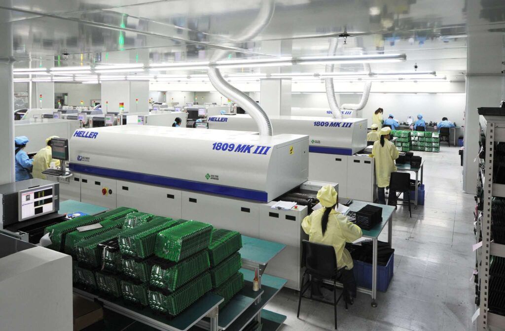
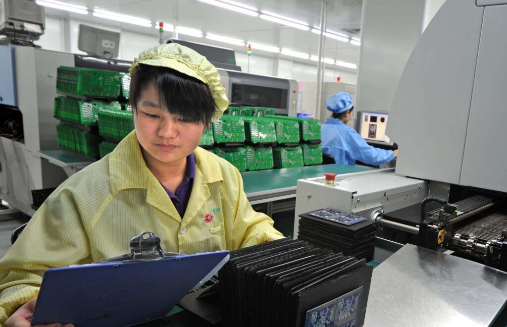
Component Assembly: Follows the bare-board fabrication, where electronic components are mounted on the board. An automated machine is usually used for this process, which picks up the component and places it on the board. The components are then soldered to the board using wave soldering or reflow soldering.
Quality Control: This is an important aspect of the PCBA manufacturing process that needs to be implemented throughout the process to ensure that the PCB meets performance requirements. Any defects found during the process need to be addressed immediately by stopping the process, exploring the cause, and finding a solution to the problem. This is critical to ensure the quality of the final product.